
Integrated Circuit (IC) Packaging Design Trends: Demands, Challenges, and the Role of EDA Tools
Introduction
As transistor scaling approaches its physical limits, the semiconductor industry is entering a new era where performance gains no longer come from shrinking nodes alone [1]. Instead, innovation is shifting to the package– the critical interface that binds multiple chips into a single, high-performance system (Figure 1). From Artificial Intelligence (AI) accelerators to automotive electronics and IoT devices, advanced packaging technologies such as 2.5D and 3D integration are enabling heterogeneous systems that deliver unprecedented power and functionality. But with these opportunities come new design complexities and sustainability pressures. For design engineers, packaging is no longer an afterthought. It directly influences power, performance, reliability, and cost– and demands a new generation of Electronic Design Automation (EDA) tools and skills to keep pace with this transformation.
This article analyses the key trends shaping IC packaging design– from miniaturization and heterogeneous integration to thermal and power delivery challenges. It also highlights how EDA tools are evolving to meet these demands and what engineers need to know to stay ahead in this rapidly changing landscape.

Figure 1: As transistor scaling slows, packaging becomes a key performance enabler.
Key Trend and Technologies
Miniaturization and High-Density Packaging
The growing demand for compact, energy‑efficient systems in mobile, edge, and embedded applications is driving a strong focus on miniaturization and high‑density packaging. As board‑level scaling reaches practical limits, advanced packaging technologies enable higher functionality within reduced form factors by increasing interconnect density and minimizing signal paths. Fan‑Out Wafer‑Level Packaging (FOWLP), as the one seen in Figure 2, is widely adopted for ultra‑thin, compact designs, offering high I/O density without the need for traditional substrates. In parallel, fine‑pitch Flip‑Chip Ball Grid Array (FCBGA) packages continue to evolve, supporting high‑performance devices that require dense routing, robust power delivery, and scalability for larger chips and multi‑chip configurations (see Figure 3).

Figure 2: Example of a Fan-out wafer level package (FOWLP).

Figure 3: Example of FCBGA package with multi-chip configuration.
While these approaches deliver significant gains in performance and integration, they also introduce tighter geometrical tolerances, increased routing complexity, and heightened sensitivity to signal integrity and manufacturability, requiring engineers to adopt more advanced package design methodologies and analysis tools. As these density‑driven constraints continue to escalate, the industry is increasingly turning to heterogeneous integration– combining multiple specialized dies within a single package– to extend performance scaling beyond what miniaturization alone can achieve.
Heterogeneous Integration
Heterogeneous integration is emerging as a cornerstone of advanced IC packaging, enabling the combination of logic, memory, RF, and increasingly photonic components within a single package. By integrating dies fabricated in different process nodes and optimized for specific functions, designers can overcome the limitations of monolithic scaling while improving performance, power efficiency, and system flexibility. Chiplet‑based architectures are a prominent example of this approach, with technologies such as Intel’s Foveros and TSMC’s CoWoS allowing multiple dies to be assembled using high‑density interconnects and advanced substrates or interposers [2]. These packaging platforms support high‑bandwidth communication between chiplets and facilitate heterogeneous systems tailored for applications such as AI acceleration, high‑performance computing, and advanced networking.
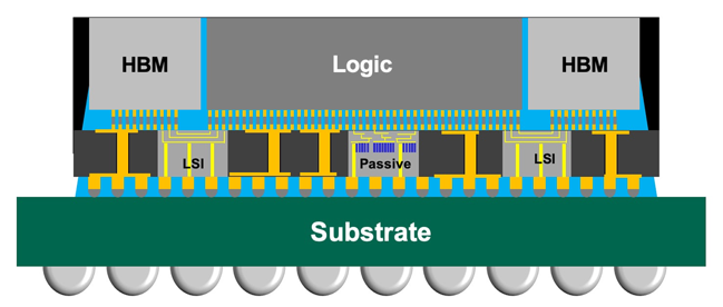
Figure 4: TSMC CoWoS technology.
However, the benefits of heterogeneous integration come at the cost of significantly increased design complexity. Electrical, mechanical, and manufacturing considerations must be addressed holistically, as interactions between different dies and interconnect technologies can have a major impact on overall system behavior. Co‑design across chip, package, and system domains becomes essential to ensure signal integrity, timing closure, and manufacturability. At the same time, concentrating diverse high‑performance components within a single package intensifies challenges related to heat dissipation and efficient power delivery. These issues make thermal management and power distribution critical factors in heterogeneous designs, naturally leading to the next focus area: thermal and power delivery challenges in advanced IC packaging.
Thermal and Power Delivery Challenges
As heterogeneous integration places multiple high‑performance dies in proximity– often stacked vertically– the demands on thermal management rise sharply. Heat generated by logic cores, memory stacks, or specialized accelerators must travel through increasingly complex material layers, which can create hotspots and local temperature gradients. These thermal non‑uniformities can degrade performance, shorten device lifetime, and complicate reliability qualification. Stacked‑die configurations, interposers, and dense redistribution layers all contribute to limited heat‑spreading paths, making traditional thermal design heuristics insufficient. To ensure safe operating margins, engineers must rely on detailed 3D thermal modeling capable of capturing interactions between dies, underfill materials, interconnect structures, and heat‑spreading components. Figure 5 illustrates a clear thermal simulation where the heat dissipation at thermal couples in a multi-die system is shown.

Figure 5: Simulating heat dissipation at thermal couples.
In parallel, power delivery networks (PDNs) become more challenging to design as package complexity increases. Multi‑layer substrates, fine‑pitch interconnects, and longer vertical current paths introduce additional resistance and inductance, making IR drop and power supply noise worst. High‑current chiplets, memory stacks, and analog/RF components all impose different PDN requirements, making co‑optimization essential to maintain stable supply voltages across the system. These interconnected thermal and power integrity issues require a shift toward advanced simulation, early‑stage design exploration, and predictive analysis. This growing complexity naturally leads to the next topic: the evolution of EDA tools—which are adapting to provide integrated thermal‑electrical analysis, 3D‑aware design environments, and chip‑package‑system co‑optimization capabilities necessary for modern IC packaging.
EDA Tool Evolution
As advanced packaging pushes integration into the third dimension, traditional 2D EDA workflows are no longer sufficient to capture the complex electrical, thermal, and mechanical interactions within modern IC packages. Designers now require 3D‑aware environments capable of handling stacked‑die placement, fine‑pitch interconnect routing, multi‑layer redistribution structures, and advanced thermal coupling effects (Figure 6). Solutions such as Ansys RedHawk‑SC for power‑thermal analysis and Cadence Celsius and Integrity 3D‑IC for integrated multiphysics and co‑design exemplify how major EDA platforms are evolving to address these challenges. These environments incorporate integrated thermal-electrical analysis tools– including thermal, power integrity, and signal integrity– to predict behavior across the full chip‑package system. In parallel, the blurring of boundaries between silicon, package, and board has accelerated the need for true chip‑package‑board co‑design, enabling engineers to evaluate trade‑offs such as interconnect density, PDN impedance, and package warpage early in the design cycle. This integrated perspective is becoming essential as package‑level choices increasingly dictate system‑level performance and reliability.

Figure 6: 3D-IC design workflow.
The shift toward heterogeneous integration also transforms engineering workflows. Instead of isolated design stages, engineers must adopt multi-domain co‑optimization flows that allow silicon architects, package designers, and system engineers to collaborate in a unified environment. This includes shared design data, synchronized electrical‑thermal simulations, and iterative exploration of placement, interconnect topology, and cooling strategies. As these workflows grow more complex, the industry is turning toward higher levels of abstraction and automation to manage design scale and reduce cycle times. This naturally sets the stage for the next major trend in advanced packaging design: digitalization and automation, where AI‑driven optimization, digital twins, and intelligent design assistants begin to reshape how complex multi‑die systems are conceived and verified.
Digitalization and Automation
As IC packaging complexity increases, design teams are turning to AI‑ and machine‑learning‑driven optimization to explore placement, routing, and thermal‑electrical trade‑offs more efficiently, reducing manual iteration and accelerating closure. In parallel, digital twin methodologies are becoming central to packaging development, providing virtual replicas that integrate electrical, thermal, mechanical, and manufacturing data to predict system behavior and reliability before hardware exists. These digital models enable earlier identification of risk factors– such as warpage, thermal hotspots, or PDN weaknesses– while supporting continuous design‑space exploration throughout the product lifecycle [3]. Together, AI‑assisted automation and digital‑twin‑based simulation are enabling faster design cycles, improved prediction accuracy, and more robust reliability assessments, setting the foundation for increasingly intelligent and automated workflows that will define the next era of advanced IC packaging design.
Outlook
The next wave of IC packaging innovation will be shaped by growing standardization and the adoption of new integration technologies (Figure 7). One of the most influential developments is the continued maturation of chiplet interconnect standards such as UCIe, which aim to provide a unified ecosystem for die‑to‑die communication and enable interoperable chiplet marketplaces. At the same time, the integration of silicon photonics, compound semiconductors, and advanced materials will expand the design space for high‑bandwidth, energy‑efficient systems. These trends signal a shift toward packaging platforms that support not only heterogeneous electrical integration but also optical data paths, broader bandwidth per watt, and new forms of 3D system assembly.

Figure 7: Evolution of packaging technologies and development flows.
As design complexity escalates, engineers will need to cultivate cross‑domain expertise that spans electrical, thermal, mechanical, and manufacturing considerations. Multi‑die systems require simultaneous awareness of power integrity, signal routing constraints, material behavior, thermomechanical stress, and assembly tolerances– areas that have traditionally belonged to separate disciplines. The growing presence of AI‑driven design tools will further reshape the engineering workflow, enabling faster exploration, guided optimization, and automated detection of risks within vast multidimensional design spaces. This evolution places a premium on the ability to collaborate across domains and interpret insights generated by increasingly intelligent design systems.
Beyond technology, regulatory and sustainability pressures will also influence the trajectory of advanced packaging. Governments and manufacturers are placing stronger emphasis on environmentally responsible materials, recyclability, and reduced energy consumption throughout the product lifecycle [3]. In parallel, sectors such as automotive, aerospace, and defense are demanding stricter reliability and qualification standards, driven by safety‑critical requirements and longer mission lifetimes. Meeting these regulatory expectations– while maintaining aggressive performance targets– will require packaging solutions that balance innovation with robust validation and lifecycle assurance. Together, these forces suggest that the future of IC packaging will be defined not only by technical breakthroughs but also by responsible engineering practices and globally aligned standards.
Conclusion
Advanced IC packaging has become a performance enabler– delivering higher bandwidth, lower latency, and better power efficiency through chiplets, 2.5D/3D integration, and co‑optimized package architectures– yet it introduces real challenges in thermal management, PDN integrity, manufacturability, and verification. Sustained progress will depend on tight collaboration across design, manufacturing, and packaging ecosystems, unifying silicon, substrate, and board decisions within shared data models and co‑design workflows. Looking ahead, 3D ICs– underpinned by standardized die‑to‑die interfaces, multiphysics‑aware EDA, and digitally orchestrated development– are poised to shape the next decade of semiconductor innovation by scaling system capability beyond the limits of traditional transistor shrink while meeting stringent reliability and sustainability expectations.
References
[1] “Packaging a Revolution: How Advanced Semiconductor Technologies are Redefining Performance” — TokenRing / FinancialContent (Oct 23, 2025)
[2] “Advanced Packaging Becomes the Next Frontier in Chip Performance, Reports DIGITIMES” — Packnode (Nov 7, 2025)
[3] “Digital Twins For Packaging: Bridging Design, Fab, Test, And Reliability” — Semiconductor Engineering (Oct 23, 2025)
